2D Materials
Seminal materials for new-generation devices
After the noble price was given “for groundbreaking experiments regarding the two-dimensional material graphene” a wide variety of 2D materials have emerged. The specific challenge with these materials is to find the right precursors enabling the deposition via CVD or an ALD process. Our R&D team is happy to accept new challenges and develop the right precursor for/with you.
01.
LED
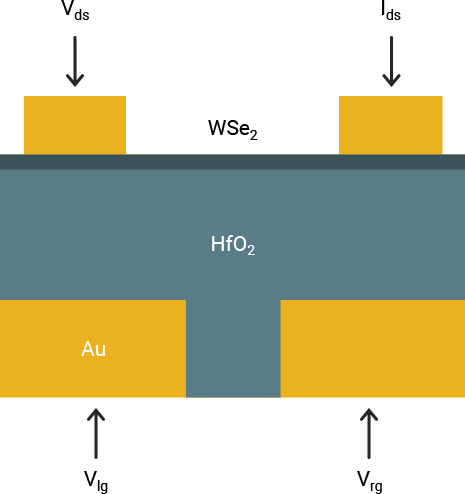
In contrast to bulk TMDCs the monolayered structures exhibit a direct band gap and can, therefore, be employed as LED. Both MoS2 and WSe2 are investigated in such devices. The doping of the 2D layer is controlled by applying the respective voltage to the left and right gates.
02.
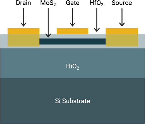
Logic Application
Since 2D layers consist of only one monolayer, they are excellent for application in flexible thin-film transistors (TFT). The first room-temperature operation was demonstrated in 2011 employing MoS2 as the semiconducting channel. Covering the MoS2 layer by HfO2 as dielectric is required to increase the carrier mobility in MoS2.