Total Quality Management
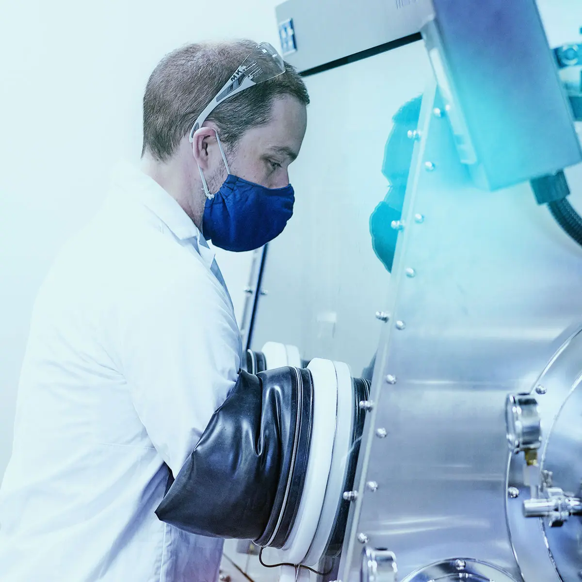
Since our foundation, our Total Quality Management System has been based on stringent ISO standards, and we hold ISO 9001:2015 and ISO 14001:2015 certifications. Our plant in Marburg/Germany has state-of-the-art production equipment and follows our strict MOCVD platform approach. Every chemical we produce which reaches semiconductor purity is handled using MOCVD approved equipment and components. In this way, we can ensure highest purity and consistency of our processes. Key to our quality system is the direct link to our customers’ processes.
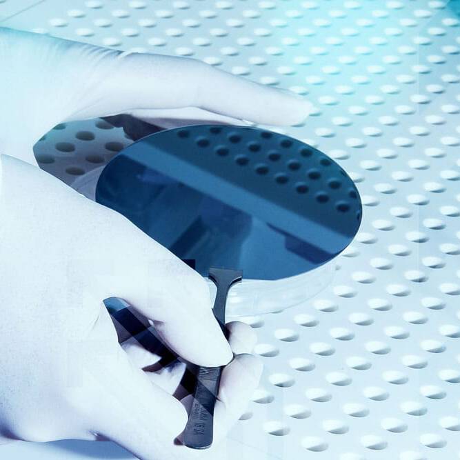
We use standard analytical methods, such as ICP-AES, ICP-MS, H-NMR, GC and others, to measure and control the purity of our precursors.
For certain products, however, we use a unique approach to quality control. As the purity of such precursors is extremely high, the detection limits of standard analytical methods are insufficient. Therefore, we deposit semiconducting layers with our precursors and analyze their properties. In general, we use epitaxy of III/V semiconductors to test the purity of certain precursors in our portfolio.
EPIGRADE™
This EPIGRADE™ qualification is a truly unique part of the DOCK Total Quality Management System. We are committed to improving our products in order to continually exceed the purity and consistency required for successful epitaxy. Our company has defined this unique service to guarantee the proven quality of each batch. Our customers benefit from reduced costs associated with qualification runs and potential downtime.
A production batch that is EPIGRADE™ is tested by means of epitaxial growth of reference material systems and test structures specifically designed to be sensitive to impurities which are affecting the electronic and optoelectronic properties. The chosen structures are either sensitive to the majority or minority carrier properties, hence enabling a complete picture of the chemicals used for deposition.
These sets of test structures are grown and characterized at an independent lab (Philipps University/Marburg) and followed by physical characterization of the deposited compound semiconductor layer structure. Characterizations routinely performed include: photoluminescence, Hall measurement and calibrated SIMS. Other characterization methods are available on request.