Phase Change-Materials
Phase change materials are investigated for more than half a decade already. In the beginning, materials based on the Te-As-Si-Ge system were too slow for memory applications. Revival came in 1987 as fast-switching devices based on compositions on the pseudo-binary line of GeTe and Sb2Te3. The first commercial application of phase-change materials was in rewritable optical storage disks such as CDs and DVDs. Yet, for a truly large-scale industrial applications for electronic memory in everyday devices some work has to be done.
As the name suggests phase-change materials exhibit at least two phases that may change upon heating through a laser or electrical current. High contrast between the optical and electrical properties of the amorphous and crystalline phases is required for optical storage or electrical storage, respectively. Crystallization time determines the writing speed and is, therefore, the data rate limiting factor. On the other hand, the amorphous phase needs high stability at the working temperature of the device.
The most widespread material applied for phase-change random access memory is Ge2Sb2Te5. Material properties can be adjusted by doping with N, O, or Sn, depending on the desired application of the device.
Working Principle of Phase-Change Random Access Memory
Extreme switching rates and the non-volatile nature of the working principle allow phase-change materials to be used in random-access memory devices and flash memory, making them an outstanding material of choice for memory application. The information is stored in the phase-change material which is connected to a control transistor (mostly field-effect transistors) in series like in dynamic random-access cells. The electrical resistance of the two phases differs by several orders of magnitude, which is used as the storage mechanism. Since the phase change is only triggered by a current pulse, the latest phase is preserved even without energy supply.
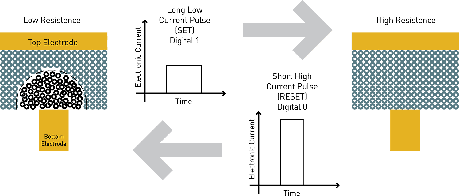
By heating the phase-change material to the crystallization temperature using a long low current pulse, the set operation is performed. Subsequently, the reset operation is performed by melting the crystalline phase with a short high current pulse and rapid cooling for amorphization. The read operation is performed by a very low current pulse. A critical device parameter is the reset current that is controlled by the access device, which determines the cell dimension and therefore limits the storage density.
Deposition and Challenges
Sputter deposition is the most common deposition method for phase-change materials. However, for more sophisticated device designs, where the phase-change material is more confined as in a mushroom-type cell, sputter processes reach their limits. Besides other deposition methods, such as electrodeposition or liquid-phase deposition, atomic layer deposition (ALD) is superior due to the ability to control the thickness at an atomic level and the extreme conformality even with complex structures, which will become handy in scaled devices.
The most challenging part of a successful atomic layer process is to find the right Te precursor. Organometallic and alkyl amide precursors exhibit poor reactivities with slow surface reactions towards each other. Hence, a plasma enhanced ALD process is required. However, no pure atomic layer deposition behavior is observed and segregation effects occurred. Alkyl silyl precursors react strongly with metal chlorides, which rendered a breakthrough for atomic layer deposition of Ge2Sb2Te5 material. Compounds with small alkyl groups (methyl or ethyl) are liquids at room temperature, have sufficient vapor pressure, thermal stability, and show a high reactivity. The ternary alloy is achieved by mixing the cycles for the binary compounds in a super cycle. The critical parameter is the ratio of the binary cycles to achieve stoichiometric Ge2Sb2Te5.
Have a look on our product finder for a range of materials to deposit phase-change materials. In case your desired molecule is not on the list just contact us!
References:
- le Gallo, M. & Sebastian, A. An overview of phase-change memory device physics. J Phys D Appl Phys 53, 213002 (2020) doi: 10.1088/1361-6463/ab7794.